Each of the eight Synergistic Processor Elements (SPEs) is a 128-bit RISC processor specialized for data-rich, compute-intensive SIMD applications.
- The Synergistic Processor Unit (SPU).
- The Memory Flow Controller (MFC).
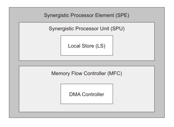
The SPU deals with instruction control and execution. It includes a single register file with 128 registers (each one 128 bits wide), a unified (instructions and data) 256-KB local store (LS), an instruction-control unit, a load and store unit, two fixed-point units, a floating-point unit, and a channel-and-DMA interface. The SPU implements a new SIMD instruction set, the SPU Instruction Set Architecture, that is specific to the Broadband Processor Architecture.
Each SPU is an independent processor with its own program counter and is optimized to run SPE threads spawned by the PPE. The SPU fetches instructions from its own LS, and it loads and stores data from and to its own LS. With respect to accesses by its SPU, the LS is unprotected and un-translated storage. The MFC contains a DMA controller that supports DMA transfers. Programs running on the SPU, the PPE, or another SPU, use the MFC’s DMA transfers to move instructions and data between the SPU’s LS and main storage. (Main storage is the effective-address space that includes main memory, other SPEs’ LS, and memory-mapped registers such as memory-mapped I/O [MMIO] registers.) The MFC interfaces the SPU to the EIB, implements bus bandwidth-reservation features, and synchronizes operations between the SPU and all other processors in the system.
To support DMA transfers, the MFC maintains and processes queues of DMA commands. After a DMA command has been queued to the MFC, the SPU can continue to execute instructions while the MFC processes the DMA command autonomously and asynchronously. The MFC also can autonomously execute a sequence of DMA transfers, such as scatter-gather lists, in response to a DMA-list command. This autonomous execution of MFC DMA commands and SPU instructions allows DMA transfers to be conveniently scheduled to hide memory latency.
Each DMA transfer can be up to 16 KB in size. However, only the MFC’s associated SPU can issue DMA-list commands. These can represent up to 2,048 DMA transfers, each one up to 16 KB in size. DMA transfers are coherent with respect to main storage. Virtual-memory address-translation information is provided to each MFC by the operating system running on the PPE. Attributes of system storage (address translation and protection) are governed by the page and segment tables of the PowerPC Architecture. Although privileged software on the PPE can map LS addresses and certain MFC resources to the main-storage address space, enabling the PPE or other SPUs in the system to access these resources, this aliased memory is not coherent in the system.
The SPEs provide a deterministic operating environment. They do not have caches, so cache misses are not a factor in their performance. Pipeline-scheduling rules are simple, so it is easy to statically determine the performance of code. Although the LS is shared between DMA read and write operations, load and store operations, and instruction prefetch, DMA operations are accumulated and can only access the LS for at most one of every eight cycles. Instruction prefetch delivers at least 17 instructions sequentially from the branch target. Thus, the impact of DMA operations on loads and stores and program-execution times is, by design, limited.