The SPE supports big-endian data ordering, an ordering in which the lowest-address byte and lowest-numbered bit are the most-significant (high) byte and bit, respectively.
Bits in registers are numbered in ascending order from left to right, with
bit 0 representing the most-significant bit (MSb) and bit 127 the least-significant
bit (LSb) as shown in the figure below. The SPE architecture does not define
or use little endian data ordering.

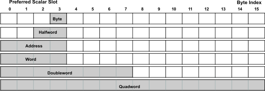
The SPU hardware defines the following data types:
- byte — 8 bits
- halfword — 16 bits
- word — 32 bits
- doubleword — 64 bits
- quadword — 128 bits
These data types are indicated by shading in Figure 2. The left-most word (bytes 0, 1, 2, and 3) of a register is called the preferred scalar slot (also shown in Figure 2).
When instructions use or produce scalar operands or addresses, the values
are in the preferred slot. A set of store assist instructions is available
to help store bytes, halfwords, words, and doublewords.
The SPE programming model defines the vector data types shown in Table 1 for the C programming language. These
data types are all 128 bits long and contain from 1 to 16 elements per vector.
| Vector Data Type | Content |
|---|---|
| vector unsigned char | Sixteen 8-bit unsigned chars |
| vector signed char | Sixteen 8-bit signed chars |
| vector unsigned short | Eight 16-bit unsigned halfwords |
| vector signed short | Eight 16-bit signed halfwords |
| vector unsigned int | Four 32-bit unsigned words |
| vector signed int | Four 32-bit signed words |
| vector unsigned long long | Two 64-bit unsigned doublewords |
| vector signed long long | Two 64-bit signed doublewords |
| vector float | Four 32-bit single-precision floats |
| vector double | Two 64-bit double precision floats |
| qword | quadword (16-byte) |